Értékelések
Nincs még értékelés. Legyél Te az első!
Mit olvastak a többiek, ha ezzel végeztek?


Tartalmi kivonat
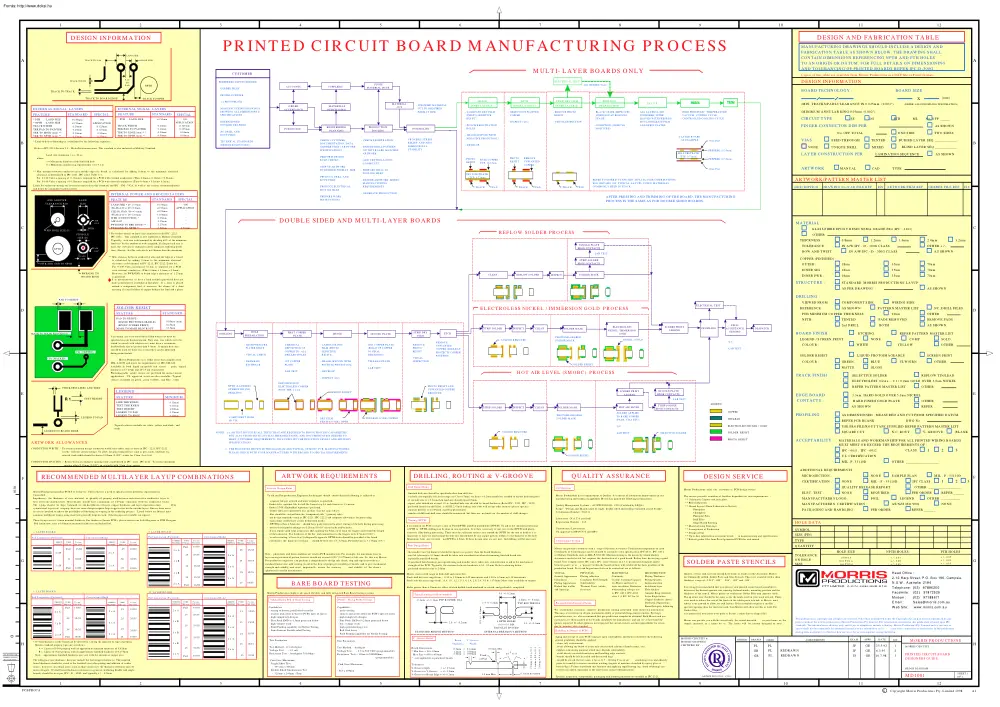
1 2 3 DESIGN INFORMATION 4 5 6 7 8 9 10 11 DESIGN AND FABRICATION TABLE PRINTED CIRCUIT BOARD MANUFACTURING PROCESS MANUFACTURING DRAWINGS SHOULD INCLUDE A DESIGN AND FABRICATION TABLE AS SHOWN BELOW. THE DRAWING SHALL CONTAIN DIMENSIONS REFERENCING NPTH AND PTH HOLES TO AN ORIGIN OR DATUM. FOR FULL DETAILS ON DIMENSIONING AND TOLERANCING OF PRINTED BOARDS REFER IPC-D-300G. LAND SIZE A TRACK TO PAD HOLE SIZE MULTI- LAYER BOARDS ONLY CUSTOMER PAD TO PAD TRACK WIDTH NPTH ACCOUNTS - GERBER FILES STORE MATERIAL ISSUE SUPPLIERS A Copies of this table are available from Morris Productions in a DXF file or Protel formats. DESIGN INFORMATION ELECTRICAL TEST PREFERRED INPUTS NEEDED 12 - EG. BURIED VIAS BOARD TECHNOLOGY : TRACK TO TRACK BOARD SIZE : - PROTEL PCB FILE TRACK TO BOARD EDGE IMAGE - 1:1 PHOTOPLOTS EXTERNAL SIGNAL LAYERS FEATURE STANDARD SPECIAL FEATURE +0.50mm +0.70mm 0.20mm 0.20mm 0.53mm 0.53mm ON APPLICATION 0.125mm 0.125mm 0.53mm 0.53mm
* PTH * PTH - LAND SIZE * NPTH - LAND SIZE TRACK WIDTH TRK/PAD TO PAD/TRK TRK TO EDGE (min) * TRK TO NPTH (min) * B STANDARD SPECIAL +0.50mm ON APPLICATION 0.125mm 0.125mm 0.50mm 0.50mm - LAND SIZE 0.20mm 0.20mm 0.50mm 0.50mm TRACK WIDTH TRK/PAD TO PAD/TRK TRK TO EDGE (min) * TRK TO NPTH (min) * ORDER ACCEPTANCE - MANUFACTURING DRAWINGS SHOWING ALL DIMENSIONS & SPECIFICATIONS INTERNAL SIGNAL LAYERS PCB DESIGN - NC DRILL AND ROUT FILES - TECHNICAL STANDARDS (DESIGN RULES USED) Refer to IPC-2221 Section 9.0 - Holes/Interconnections This standard is also endorsed as Military Standard Land size, minimum = a + 2b +c a = Maximum diameter of the finished hole b = Minimum annular ring requirements ( see 9.12) - CHECK CUSTOMER DOCUMENTATION, DATA, GERBER FILES / ARTWORK SPECIFICATIONS - CHECK REGISTRATION - PRODUCE DRILL AND ROUT FILES Lands for surface mounting are covered extensively in this Standard and IPC - SM - 782A, as well as the various recommendations laid down
by component manufacturers. - PRODUCE ELECTRICAL TEST JIG FILES FEATURE LAND SIZE AIR GAP WEB INNER LAYER(S) - ENSURE DRILL PATTERN ON TEST BOARD MATCHES ARTWORK INNER LAYER(S) - LAMINATE DRY FILM (PHOTO SENSITIVE RESIST) AIR GAP PRESSING INNER LAYER(S) NORMALISE LAY-UP PREPARATION - BLACK OXIDE (IMPROVES ADHESION AT BONDING STAGE) - REMOVE UNWANTED COPPER - REMOVE PHOTO RESIST - INSPECT ( Q.C) - VISUAL INSPECTION - CONDITION ( REMOVE MOISTURE) - PUNCH REGISTRATION HOLES (MIN. TRACKS/PADS/CLEARANCE IN 0025mm (0001") CIRCUIT TYPE : PWR/GND TO BOARD EDGE DS PTH ML No. OFF AS SHOWN No. OFF TOTAL 4 LAYER BOARD AS EXAMPLE VIAS : 18um Foil - DEVELOP NONE ONE SIDE TWO SIDES FEED THROUGH TENTED BURIED LAYER SEQ UNIQUE DRILL MIXED BLIND LAYER SEQ B PREPREG (0.35mm) PHOTO RESIST - ADD VENTING, LOGOS CODING ETC. PHOTO RESIST BASE COPPER TYP. 18/35um FR4 SUBSTRATE (TYP. 071mm) REMOVE UNWANTED COPPER LAYER
CONSTRUCTION PER : ARTWORK : FR4 SUBSTRATE (TYP. 071mm) - ENSURE ARTWORK MEETS MANUFACTURING REQUIREMENTS TRACK PAD PAD TRACK LAMINATION SEQUENCE AS SHOWN PREPREG (0.35mm) 18um Foil - PREPARE FINAL NC TOOLING FILES SPECIAL +0.50mm +0.55mm +0.90mm +1.00mm 0.25mm 0.25mm 1.27mm 0.50mm ON APPLICATION " " " " " 0.50mm PAD TRACK MANUAL CAD TYPE ARTWORK/PATTERN MASTER LIST REFER TO MORRIS' STANDARD MULTI-LAYER COMBINATIONS FOR DETAILS ON TYPICAL LAYUPS USING MATERIALS COMMONLY HELD IN STOCK. DESCRIPTION DRAWING No./CAD FILE REF ISS ARTWORK/FILM REF GERBER FILE REF ISS AFTER PRESSING AND TRIMMING OF THE BOARD, THE MANUFACTURING PROCESS IS THE SAME AS FOR DOUBLE SIDED BOARDS. DOUBLE SIDED AND MULTI-LAYER BOARDS MATERIAL : C GLASS FIBRE EPOXY RESIN NEMA GRADE FR4 (IPC - 4101) REFLOW SOLDER PROCESS OTHER NI/GOLD PLATE EDGE CONTACTS * Min. distance between conductive area and the edge of a board is calculated by adding 0.4mm to the
minimum electrical clearance as determined in IPC-2221, IPC-2222. Table 6-1 For 0-100 Volts a spacing of 0.1mm is required for a PCB with internal conductors. (Thus 04mm + 01mm = 05mm) However, for PWR/GND to board edge a clearance of 1.27mm is preferred. It is not necessary to have a land around a pin which does not make connection to anything on that plane. If a land is placed around a component lead, it increases the chance of a short occuring if a small slither of copper bridges the land and a plane PWR AND GND TO NPTH SS FINGER CONNECTOR DIM PER : REFLOW SOLDER SOLDER MASK INSPECT 0.8mm TOLERANCE : IN A/W IPC - D - 300G CLASS 1.2mm 2.4mm 1.6mm 3.2mm OTHER + / - IN A/W IPC - D - 300G CLASS AS SHOWN COPPER (FINISHED) : STRIP SOLDER EDGE CONTACTS CLEAN THICKNESS : BOW AND TWIST : - LAB TEST LAND SIZE (REFER ALSO PROFILING INFORMATION) (MINIMUM ANNULAR RING 0.05mm (0002") - HIGH PRESSURE/ TEMPERATURE VACUUM CURING CYCLE - CONTROLLED COOLING CYCLE - ALL
LAYERS LAID TOGETHER, INTERLEAVED WITH PREPREG, MOULD RELEASE FILM AND PRESS PLATES. - IMAGE (EXPOSE WITH NEGATIVE PHOTOTOOL) - PROVIDES STRESS RELIEF AND AIDS DIMENSIONAL STABILITY * For further details on land size calculations refer IPC -2221 IPC-2222. This standard is also endorsed as Military Standard Typically, web size is determined by dividing 60% of the minimum land size by the number of webs required. If a larger land size is used, the web size is reduced to allow adequate soldering dwell time. (Ensure that the web size is not thinner than the minimum FIN HOLE SIZE (D) STRIP DRY FILM - PREPARE WORK INSTRUCTIONS STANDARD LAND SIZE * D<=3.0mm (Fin Hole D+) D>=3.0mm CLEAR. PAD *D<=3.0mm (Fin Hole D+) D>=3.0mm WEB (CONDUCTOR) * AIR GAP PWR/GND TO BRD EDGE * PWR/GND TO NPTH * - SPECIFIED MATERIAL CUT TO REQUIRED FORMAT SIZE ETCH - GENERATE PRODUCTION INTERNAL POWER AND GROUND LAYERS NPTH PRODUCTION TOOLING - STEP UP ARTWORK TO DESIRED FORMAT SIZE * Min.
distance between conductive area and the edge of a board is calculated by adding 04mm to the minimum electrical clearance as determined in IPC-2221, IPC-2222. Table 6-1 For 0-100 Volts a spacing of 0.13mm is required for a PCB with external conductors (Thus 04mm + 013mm = 053mm) For 0-100 Volts a spacing of 0.10mm is required for a PCB with internal conductors (Thus 04mm + 01mm= 05mm) FIN HOLE SIZE (D) ENGINEERING PLANNING - PERFORM DESIGN RULE CHECKS where: C MATERIALS PURCHASING - DIMENSIONED OUTLINE DRAWING * Land-to-hole relationship is established by the following equation: GND AND PWR CLEARANCE PAD MATERIAL CUT (mm) X TRACK TO NPTH OUTER : 18um 35um 70um INNER SIG : 18um 35um 70um INNER PWR : 18um 35um 70um STRUCTURE : STANDARD 'MORRIS PRODUCTIONS' LAYUP AS PER DRAWING AS SHOWN DRILLING : PAD TO RESIST D ELECTROLESS NICKEL / IMMERSION GOLD PROCESS STANDARD FEATURE PAD TO RESIST:(LIQUID PHOTOIMAGEABLE) (EPOXY SCREEN PRINT) MASK TO MASK
BLOCKOUT NPTH : 0.05mm (min) 0.25mm 0.15mm STRIP SOLDER HOLE PREPARATION DRILLING Vias which are to be tented &/or filled with resist must be specified in your documentation. Note also, vias which are to be tented (covered) with solder resist, must have a maximum finished hole size no greater than 0.6mm A unique hole size should be used for these vias so that they can be identified during manufacture. VIA (MASKED) - HIGH PRESSURE WATER RINSE INSPECT CLEAN - 2ND COPPER PLATE (BUILD UP COPPER TO FINAL THICKNESS) - DESMEAR/ ETCHBACK - 1ST COPPER PLATE - IMAGE (EXPOSE WITH POSITIVE PHOTOTOOL) - TIN/LEAD PLATE SOLDER MASK ETCH - PHOTOIMAGEABLE SOLDER MASK - REMOVE UNWANTED COPPER (TIN/LEAD PROTECTS COPPER PATTERN) - REMOVE PHOTO RESIST SCREEN PRINT LEGEND ELECTROLESS NICKEL / IMMERSION GOLD PROFILING WIRING SIDE PATTERN MASTER LIST ETCHING REFER PATTERN MASTER LIST NONE COMP. SOLD. - Q.C WHITE SOLDER RESIST : - VISUAL INSPECTION COLOUR : YELLOW OTHER
LIQUID PHOTOIMAGEABLE GREEN BLUE MATTE GLOSS SCREEN PRINT YLW/GRN OTHER SOLDER RESIST HOT AIR LEVEL (SMOBC) PROCESS TRACK FINISH : SELECTIVE SOLDER REFLOW TIN/LEAD ELECTROLESS Ni/Au - 0.1 / 02um GOLD OVER 30um NICKEL DEPOSITION OF ELECTROLESS COPPER NOM. THK 20 um PHOTO RESIST AND UNWANTED COPPER REMOVED PHOTO RESIST REFER PATTERN MASTER LIST SCREEN PRINT LEGEND DRY FILM TENTS(COVER) NPTH INSPECT CLEAN HOT AIR LEVEL SOLDER MASK - PHOTOIMAGEABLE SOLDER MASK TIN/LEAD OVER COPPER Typical colours available are white, yellow and black ; and made SOLDER REMOVED NOTES. 1: LAB TEST INCLUDES ALL TESTS THAT ARE REQUIRED TO PROVE PROCESS CAPABILITIES, BUT ALSO THOSE TESTS (SUCH AS MICROSECTIONS), AND DOCUMENTATION NEEDED TO MEET CUSTOMER REQUIREMENTS INCLUDING IPC CERTIFICATION LEVELS AND MILITARY SPECIFICATIONS. CONDUCTOR WIDTH : - To obtain minimum design conductor width refer tables such as those in IPC - 2221, IPC-2222 for the relevant current ratings. To allow for
processing effects such as pits, nicks, undercut etc, artwork track width should be drawn 0.05mm (0002") wider for 35um (1oz) foil AS SHOWN - LAB TEST STRIP SOLDER ARTWORK ALLOWANCES REMOVE PADS BOTH BOARD FINISH : NI/GOLD PLATE EDGE CONTACTS EDGE BOARD CONTACTS : - LAB TEST LEGEND TO BOARD EDGE PADS REMOVED 2nd DRILL COLOUR : - DEVELOP COMPONENT HOLE 0R VIA D OTHER DESPATCH - INSPECT (Q.C) 0.15mm 0.15mm 1.00mm 0.25mm 0.25mm NC DRILL FILES 20um TENTED LEGEND / SCREEN PRINT : NICKEL / GOLD MINIMUM LINE THICKNESS TEXT THICKNESS TEXT HEIGHT LEGEND TO PAD LEGEND TO EDGE LEGEND TO PAD - VISUAL CHECK - LAMINATE DRY FILM (PHOTO SENSITIVE RESIST) NPTH (LANDLESS OTHERWISE 2ND DRILLING) FEATURE SECOND PLATE - CHEMICAL DEPOSITION OF COPPER TO ALL DRILLED HOLES - LAB TEST LEGEND TEXT HEIGHT IMAGE STRIP DRY FILM FINAL ACCEPTANCE TESTING - LAB TEST THICKNESS LINES AND TEXT R1 FIRST COPPER PLATE SOLDER REMOVED Morris Productions uses solder resist
that complies with MIL-I-46058 and meets the requirements of IPC-SM-840. Available in both liquid imageable and screen print, typical thickness is 15-20um and 20-25 um respectively. Photoimageable solder resists are preferred for surface mount applications. UL approved resists are also available Typical colours available are green, green / yellow, and blue : other E COMPONENT SIDE AS SHOWN PTH MINIMUM COPPER THICKNESS : MASK TO MASK BLOCKOUT VIA (TENTED) VIEWED FROM : REFERENCE : ELECTRICAL TEST SOLDER RESIST OTHER E 1.3um HARD GOLD OVER 50um NICKEL HARD FINISH GOLD PLATE OTHER AS SHOWN REFER LEGEND STRIP SOLDER EDGE CONTACTS - SOLDER APPLIED TO BARE COPPER (PADS, VIAS ETC) COPPER - Q.C ELECTROLESS NICKEL / GOLD USE PROFILE/ROUT TAPE SUPPLIED REFER PATTERN MASTER LIST SOLDER RESIST SQUARE CUT - LAB TEST PROFILING : TIN/LEAD SELECTIVE SOLDER AS DIMENSIONED , MEASURED AND CUT FROM SPECIFIED DATUM. DWG No. REFER PCB BLANK PHOTO RESIST ACCEPTABILITY : 2 : THE
PROCESSES SHOWN IN THIS DIAGRAM ARE TYPICAL OF MOST PCB MANUFACTURERS. PLEASE CHECK WITH YOUR MANUFACTURER WITH REGARD TO SPECIAL REQUIREMENTS. N.C ROUT BLANK MATERIALS AND WORKMANSHIP FOR ALL PRINTED WIRING BOARDS MUST MEET OR EXCEED THE REQUIREMENTS OF : CLASS IPC - 6011, IPC - 6012 SOLDER RESIST V- GROOVE 1 2 3 U.L CERTIFICATION MIL -P- 55110D CONDUCTOR SPACING : - Refer electrical conductor spacing table as published in IPC -2221, IPC-2222 . To ensure minimum spacing allow 0.05mm (0002") on artworks with 35um (1oz) copper OTHER ADDITIONAL REQUIREMENTS : RECOMMENDED MULTILAYER LAYUP COMBINATIONS To aid our Pre-production Engineers the designer should ensure that the following is adhered to : - These layups are for 1.6mm nominal thickness For thicker or thinner PCB's, please contact our Sales Engineer or PCB Designer Foil lamination uses a 0.05mm maximum thickness resin backed foil 8 LAYER BOARD 18/00 CORE THK(mm) .25 * SHEETS PREPREG
Cu (um) PER SIDE 18/00 35/35 35/35 18/00 18/00 .25 SHEETS PREPREG .25 35/35 .18 35/35 2xA .18 35/35 2xA Foil 18/00 1xB 6 LAYER BOARD * SHEETS PREPREG Conventional Build CORE THK(mm) Cu (um) PER SIDE Foil 18/00 .38 0 CORE THK(mm) Cu (um) PER SIDE .15 18/00 .25 35/35 * SHEETS PREPREG 35/35 .25 35/35 .25 35/35 35/35 18/00 Cu (um) PER SIDE Foil 18/00 SHEETS PREPREG .15 35/35 .15 35/35 .15 18/00 .15 35/35 * Overall thickness of the board can be altered by varying the quantity & type of prepreg. Morris standard prepreg types are as follows: A = 1 piece of 1080 prepreg with an approximate finished thickness of 0.07mm B = 1 piece of 7628 prepreg with an approximate finished thickness of 0.175mm Note - approximate finished thickness can vary with the amount of copper area. Cu (um) PER SIDE .15 35/35 .15 35/35 .15 35/35 2xA 2xA 1xB .15 .15 2xA Foil 35/35 .15 18/00 35/35 2 3 2.4mm +/- 01mm TYP ROUTER DIA 2.4mm +/- 01mm
TYP ROUTER DIA Capabilities - netlist testing - analyse and create netlist for PCB's upto 24 layers - high complexity designs - Fine Pitch SMD to 0.25mm pitch and below - low volume work - high speed discharge test - Ball Grid Array - Fault Finding capability for Netlist Testing 2.0 +/- 02mm V - Groove Detail Test Parameters Test Method - 12 volt digital Voltage Test - 12 volt Resistance Test - breakpoint 70 kOhms Test Method - Analogue Voltage Test - 0.5 to 500 VDC (programmable) Resistance Tests - 1Ohm to 500MOhms (programmable) Board Dimensions 0.8mm = 016mm * Min Size = 80 x 80mm 1.6mm = 050mm 2.4mm = 080mm Max Size = 400 x 400mm * - not applicable to panelised boards Card Size (Maximum) Tolerances V-Groove depth = +/- 0.1mm V-Groove to V-Groove = +/- 0.2mm V-Groove to Board Edge = +/- 0.2mm 4 - 863 x 609mm 5 4 NPTH HOLES 0.6 to 08 DIA EQUALLY SPACED 0.8 +/- 01mm Board Thickness V -Groove Width 0.5 mm Min Track or Pad 3.5 mm Min 45 +/- 5 PHYSICAL Plating
adhesion Conductor Peel Strength Solderability Thermal Stress (solder float test) ELECTRICAL Continuity Current Carrying Capacity Co-Planer and layer to layer insulation. Dielectric withstanding voltage test to IPC -6011, IPC-6012 class 3 (1 KV DC for 30 MICROSECTION Plating Thickness Plating Quality Interconnection hole/inner layer Hole Quality Annular Ring (internal) Layer Registration Copper thickness (inner) Dielectric Separations Pre-production Integrity Checks Board Integrity following We recommend customers approve production tooling generated from their own information. This may reveal errors in design, manufacturability or potential design improvements. For large production runs, we also recommend that pre-production samples be obtained. Both Morris and our customers are then assured of the boards suitability for manufacture, and can see at first hand the quality expected. If either option is not requested the customer must accept responsibility for errors due to incorrect
data supplied. Aging and storage of your PCB's impacts upon solderability and flatness therefore the following general guidelines should be applied: - clean, tidy environment, - avoid allowing the board to come into contact with silicones (hand creams, etc), sulphur -containing material which may degrade solderability. - avoid abrasive materials,moisture and handling edge contacts. - boards should be left in sealed and dessicated bags - should be stoved flat for a min. 6 hrs at 115 - 120 deg C in an air circulating oven immediately prior to assembly to remove moisture wicking (ingress of moisture absorbed by epoxy glass at board edge). Failure to perform this function and applying rapid heating (eg hand soldering) can result in localised separation of the inner layer surfaces(delamination). 8 PER ORDER FOIL LEGEND MANUFACTURER'S CERTIFICATION : 2 F 3 REFER OTHER AS/NZS ISO 9001 PER ORDER NONE REFER HOLE DATA SYMBOL SIZE (FIN) TYPE HOLE
SIZE TOLERANCE ON HOLE SIZE SOLDER PASTE STENCILS NPTH HOLES 0 TO 0.8 0.81 TO 16 1.61 TO 50 Morris can provide you with the stencil only, the stencil mounted in your frame, or, the stencil mounted in a frame by us. The frame will be custom designed to your ORDER DRAWN CHKD PL GR PL PL GR PL + / - 0.05 + / - 0.05 + / - 0.10 G Head Office : 2-12 Harp Street, P.O Box 196, Campsie, N.SW, Australia 2194 Telephone: (02) 97896200 Facsimile: (02) 97872529 Modem: (02) 97188671 Email : Sales@morris.comau Web Site: www.morriscomau Quality, service and fast turn around have made us leaders in the Australian Market for Chemically milled Solder Paste and Glue Stencils. These are available with a shim thickness range of 0.010", 008" , 006", 005" and 004" . It is strongly recommended that you contact your printed circuit board assembler to determine the desired aperture size opening, fiducial marks, mounting position and the thickness of the stencil. Morris
prefers to work from Gerber Files and aperture table The ap erture size should be the same as for the lands used on your track artwork. There is no need to reduce the size of the lands on the solder paste artwork, as Morris must reduce your artwork to allow for etch factors. If the assembler requires a smaller aperture opening than the land size used, then Morris will allow for this as well. For Gerber files, it is preferred if you create your pads as flashes ( rather than as shape fills). MORRIS CIRCUITS & MORRIS GRAPHICS CERTIFIED BY : - PTH HOLES + / - 0.03 + / - 0.05 + / - 0.08 This publication is copyright and all rights are reserved. Other than as permitted under the Copyright Act, no part may be reproduced by any process without the written permission of Morris Productions Pty Limited. The information contained in this publication is based upon IPC standards. The information is advisory only and its use or adaption is entirely voluntary Morris Productions Pty Limited and
its servants or agents shall not be responsible for continued currency of the information or fo r any errors, omissions or inaccuracies in this publication arising from negligence or otherwise howsoever or for any consequense arising therefrom. EXAM APPD DATE ISS JF GE 25.592 1 REDRAWN JF GE 6.395 2 REDRAWN JF GE 10.798 3 AMENDMENTS MORRIS PRODUCTIONS H MORRIS CIRCUITS PRINTED CIRCUIT BOARD DESIGNERS GUIDE BLOCK DIAGRAM 0.1 max deviation 7 1 OTHER REQUIRED PACKAGING AND HANDLING : MIL - P - 55110D IPC CLASS QUANTITY 9 SHEET 1 OF 1 MD1001 AS/NZS ISO 9001 : 1994 Specific inspection, acceptability, packaging and handling methods are detailed in IPC-2221, 6 NONE MANUFACTURER'S LOGO : Handling & Storage of PCB's INTERNAL BREAKOUT METHOD STANDARD BRIDGE METHOD Test Parameters Card Size (Maximum) Single Sided Test - 488 mm x 406mm Double Sided Simultaneous Test - 325mm x 244mm (Top) VISUAL General Appearance
Cleanliness Plating Appearance Etched line widths and Spacings. 5.0 +/- 02mm Typical routing breakout methods Probot - Flying Probe Testing 2.5 +/- 02mm Capabilities - testing to known good board or netlist - analyse and create netlist for PCB's upto 24 layers - high complexity designs - Fine Pitch SMD to 0.5mm pitch and below - high volume work - Fault Finding capability for Netlist Testing - Simultaneous Double sided Testing Morris can provide customers with a range of Quality Assurance Certifications dependent on need. Certificates of Conformance can be attained to customer's own specification, IPC-6011, IPC -6012 or Military Standards such as MIL-P-55110D. Microsectioning is the means by which Quality Assurance can be tested but requires the destruction of a good board. Rather than destroying a good board, Test Coupons (refer IPC-2221, IPC -2222 Section 12.431) positioned alongside and/or between pairs ( or as a "popout" within the board outline) will
exhibit all the basic qualities of the production board. Tests and Inspections that can be carried out are as follows:- - the smallest rout bit diameter should be equal to or greater than the board thickness - rout bit tolerance(+/-0.1mm) should be taken into consideration when determining finished board size especially panelised boards - if panelised then breakout point positioning and number must taken into consideration to aid in the mechanical strength of the PCB. Typically the distance between breakouts is 50 - 80 mm Refer to drawing below - preferred router bit size is 2.0mm Holes greater than 6.50mm are either stitched drilled, hand machined or routed, and preferably nonplated 35/35 2xA The fibreglass core thickness does not include the foil (copper thickness). The required board thickness should be stated as the finished size (after plating and addition of solder resist), however, in critical areas, such as edge connectors, the thickness tolerance may be more stringent .
Overall board thickness tolerances in general, (including double and single boards) should be in as per IPC - D - 300G, and typically + / - 0.2mm 1 CORE THK(mm) 2xA 1xB 2xA Foil CORE THK(mm) Conformance Testing Morris stocks a full range of both drill and router bits. Stock drill bit sizes range from : 0.35 to 320mm in 005 increments and 330 to 65mm in 010 increments Stock rout bit sizes range from : 0.8, 10, 12, 15, 16, 18, 20, 24, 30 & 3175mmOther sizes available on request BARE BOARD TESTING Viking Digital Bed of Nails Testing 1xB .25 35/35 Conventional Build 2xA 4xA .38 2xA * SHEETS PREPREG 35/35 1xB PCBPRO7A .25 Note - phototools and their condition are vital to PCB manufacture. For example, the maximum layer to layer misregistration of pattern features should not exceed 0.003" (0075mm) at full size In this way Morris Pre-production engineers can perform a comprehensive design rule check, step and repeat artwork to a standard format size, add venting
(to aid in the flow of prepreg for multilayer boards, and to give mechanical strength and stability) and most importantly, ensure the accuracy and stability of the diazo's (phototools) used in manufacture. Morris Productions employs advanced, flexible and fully integrated Bare Board testing systems. Foil Lamination (Preferred) 2xA 2xA DO NOT SCALE 35/35 10 LAYER BOARD Foil Lamination (Preferred) H Cu (um) PER SIDE 2xA 18/00 2xA CORE THK(mm) The service provides a number of facilities dependent on your requirements : * Schematic Capture and laser plots * Bill of Materials * Board Layout (From Schematic or Netlist) - Photoplots - Checkplots - Photoplot Files - Drill Files - Shape Based Routing * Manufacturing Drawings * Arrangement of Production * Design advice * Up to date information on current trends in manufacturing and specifications * Extract gerber files from Protel generated PCB files and amend Rout Design Rules 1xB 2xA Foil Foil .18 .50 2xB Cu (um) PER
SIDE 2xA 2xA .71 Conventional Build CORE THK(mm) Underwriters Laboratories UL approval to MP194V-0 and MP-2 2.4mm = 06 +/-01 * SHEETS PREPREG Quality Management Systems - AS/NZS ISO9001: 1994 (Certified by LRQA) Scope - "Design and Manufacture of single, double sided and multilayer printed circuit boards". Certification Number : 926131 SAMPLE PLAN MIL - P - 55110D NONE QUALITY RELEASE REPORT ELEC. TEST : Morris Productions has a committment to Quality. As a means of continuous improvement in our manufacturing and technical capibilities Morris has gained the following certifications: NONE MICROSECTION : Morris Productions offer our customers a PCB design service. Laboratory (N.ATA certified) Registration Number : 365 Tenting (NPTH) It is common for PCB's to have a mix of Plated(PTH) and Non-plated holes(NPTH). To aid in the positional tolerance of PTH to NPTH, drilling can be done in one operation. It is then necessary to tent (cover) the NPTH with
photosensitive film during processing There must be sufficient surface area around the NPTH for the tent to hold so it is important to have no land around the hole nor should there be any copper pattern within 2 x the diameter of the hole. Maximum hole size for tenti ng NPTH is 4.5mm If these design rules are not met, 2nd drilling will be necessary 1.6mm = 05 +/-01 Foil Cu (um) PER SIDE 2xB G Foil Lamination (Preferred) Conventional Build CORE THK(mm) - separate file per artwork and layer sequence is specified. - Gerber files, aperture file & drill file formats eg.2,4 inch format or 3,3 metric - Gerber 274X (Embedded Apertures) preferred - Gerber files are registered to one another ( has the same offset). - files should be viewed from the "component side " (primary side). - use design standards (such as IPC-2221, IPC-2222) and adequate allowances for processing. - each corner should have corner delineation marks. - NPTH less than 6.5mm dia should have pads
removed to allow tenting of the hole during processing - ensure that legend markings are 0.25mm (0010") from lands and/or holes - if you require gold edge connectors add a plating bar 5mm away from the fingers and extend the length of the connector. The thickness of the bar and connections to the fingers to be 05mm (0020") - to aid in routing, at least two(2) diagonally opposite NPTH holes should be provided at the board extremities, the diameter of which should be between 2.5 - 60mm Preferred size is 3175mm (1/8") Certifications - finished hole size should be specified rather than drill size - via hole size typically fall in the range of 0.3 to 07mm( via holes < 02mm should be avoided to ensure hole integrity) - if via hole size is < 0.2mm then land size should equal 05mm - aspect ratio should not exceed 1:8 ie. finished hole size divided by board thickness (Refer IPC - 2221, IPC - 2222) - preferred format for drill files is ASCII 2,4 inch leading zero's
but will accept other formats (please specify) - separate drill fil es for Plated and Non-plated holes - number of different drill sizes should be minimised, but there are no limits on the number of drill changes 0.8mm = 04 +/-01 * SHEETS PREPREG DIMENSIONS IN MILLIMETRES Drill Design Rules Artwork Design Rules Foil Lamination (Preferred) DESIGN SERVICE CERTIFICATION : Morris Productions produce PCB'S to 24 layers . Unless there is a need to specify certain dielectric separations(eg Controlled Impedence), the thickness of core material or quantity of prepreg used between each successive conductive layer is best left to the manufacturer. Most boards should have a minimum of 009mm separation between conductive layers The layup should be kept balanced i.e the distribution of layers, copper thickness, and layer separations shou ld be symmetrical to prevent warping, however some designs require large copper areas on the outside layers. Ensure these areas are cross- hatched to
reduce the possibility of blistering or warping in the soldering process. Listed below are Morris' most common multilayer layups using materials generally kept in stock. Other layups are available on request 4 LAYER BOARD QUALITY ASSURANCE DRILLING, ROUTING & V-GROOVE 0.5 +/- 01mm F mm ARTWORK REQUIREMENTS 10 11 12 C Copyright Morris Productions Pty. Limited 1998 A1