Please log in to read this in our online viewer!
Please log in to read this in our online viewer!
No comments yet. You can be the first!
What did others read after this?


Content extract
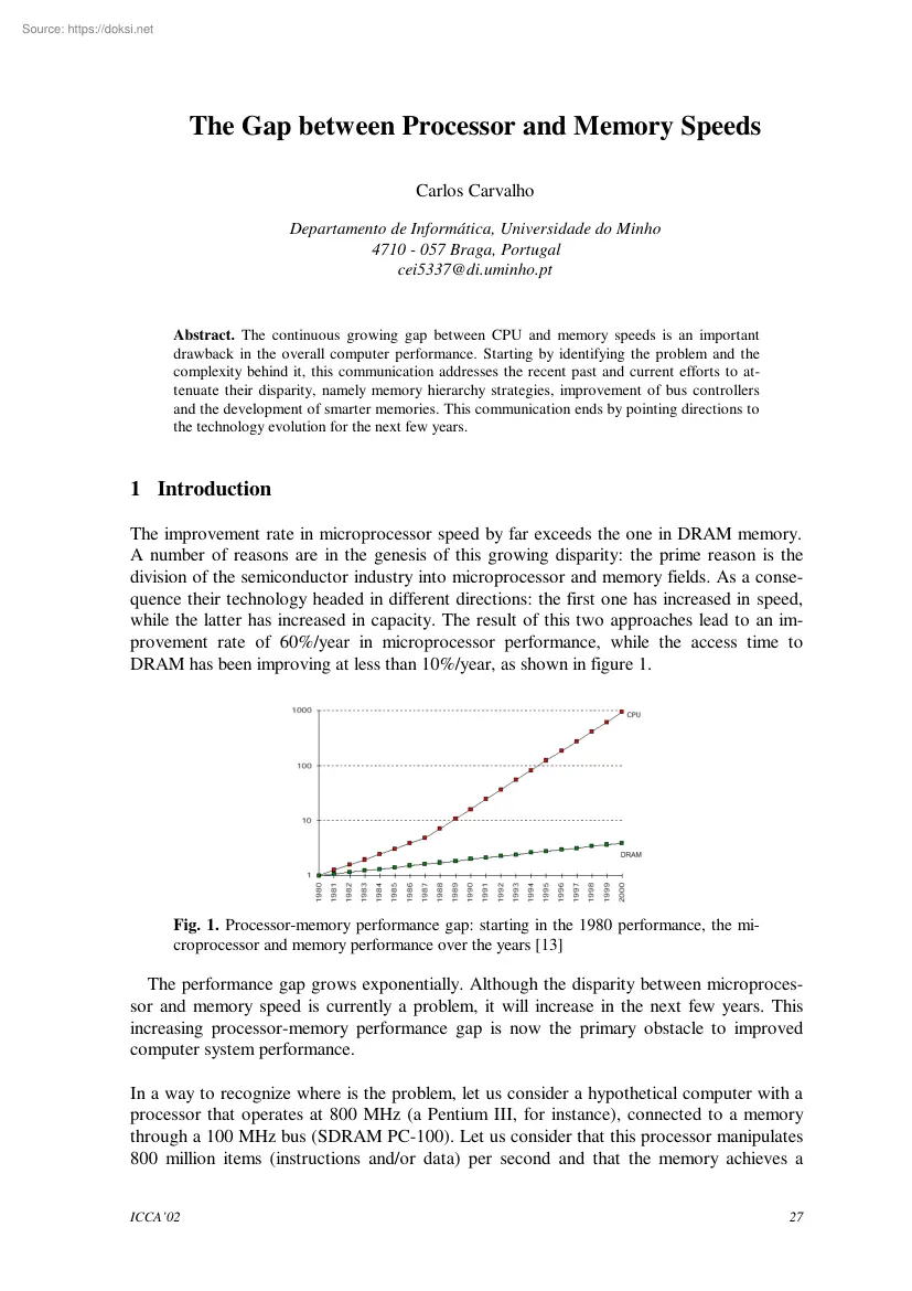
The Gap between Processor and Memory Speeds Carlos Carvalho Departamento de Informática, Universidade do Minho 4710 - 057 Braga, Portugal cei5337@di.uminhopt Abstract. The continuous growing gap between CPU and memory speeds is an important drawback in the overall computer performance. Starting by identifying the problem and the complexity behind it, this communication addresses the recent past and current efforts to attenuate their disparity, namely memory hierarchy strategies, improvement of bus controllers and the development of smarter memories. This communication ends by pointing directions to the technology evolution for the next few years. 1 Introduction The improvement rate in microprocessor speed by far exceeds the one in DRAM memory. A number of reasons are in the genesis of this growing disparity: the prime reason is the division of the semiconductor industry into microprocessor and memory fields. As a consequence their technology headed in different directions: the first
one has increased in speed, while the latter has increased in capacity. The result of this two approaches lead to an improvement rate of 60%/year in microprocessor performance, while the access time to DRAM has been improving at less than 10%/year, as shown in figure 1. Fig. 1 Processor-memory performance gap: starting in the 1980 performance, the microprocessor and memory performance over the years [13] The performance gap grows exponentially. Although the disparity between microprocessor and memory speed is currently a problem, it will increase in the next few years This increasing processor-memory performance gap is now the primary obstacle to improved computer system performance. In a way to recognize where is the problem, let us consider a hypothetical computer with a processor that operates at 800 MHz (a Pentium III, for instance), connected to a memory through a 100 MHz bus (SDRAM PC-100). Let us consider that this processor manipulates 800 million items (instructions and/or
data) per second and that the memory achieves a ICCA’02 27 debit (sending or receiving) of 100 million items per second. In this computer, for each single memory access, 8 processor clock cycles have elapsed This way 7 in each 8 clock cycles are wasted, waiting for items That represents a very high cost Although the real operation is much more complex, this example point up the existent discrepancy among the processor and memory speeds. The actuality costs, resultant from memory accesses, raise 150 clock cycles that can be compared to the 8 to 32 of the nineties minicomputers and workstations [9]. The performance of the processor-memory interface is characterized by two parameters: the latency and the bandwidth. The latency is the time between the initiation of a memory request, by the processor, and its completion In fact the problem of the increasing divergence between the memory and processor speeds is a latency growing trouble. The bandwidth is the rate at which information
can be transferred to or from the memory system. Maximum performance is achieved by zero latency and an infinite bandwidth, which characterizes the ideal memory system. It exists a close and subtle relationship among the bandwidth and the latency that is explored in the sense of improving the performance of the memory hierarchy. In the past, researchers have focus on memory latency because it has been growing relative to processor clock cycles. There are two major classes of techniques to reduce the impact of long memory latencies: latency reduction and latency tolerance Latency reduction decreases the time between the issue of a memory request and the return of the needed operand. Latency tolerance involves performing other computation while a memory request is being serviced, so that the memory latency for that request is partially or completely hidden. This will be covered in the next section. The use and success of these techniques expose the bandwidth limitations [4], since they
speedup the instructions rate, and consequently the necessity of operands also grows; they require more items than are effectively needed increasing the absolute amount of memory traffic. The bandwidth incapability slows the response times to the processor requests, ie increases the latency. Given the complex interactions between memory latency and bandwidth, however, it is difficult to determine whether memory-related processor degradation is due to raw memory latency or from insufficient bandwidth (which also increases the latency). More recently, Cuppu et al. [5] indicate that the DRAM industry invested some efforts that significantly improved bandwidth, such as synchronous DRAM (SDRAM), enhanced SDRAM (ESDRAM), double data rate DRAM (DDR), and Rambus DRAM (RDRAM); these will be considered in section 3. Section 4 brings a more radical approach that merges logic with storage capacities, as began a few years ago. The goal of these smart memories aims a simultaneous reduction of
latency and increase of bandwidth [2]. Last section makes some considerations on the possible options of evolution of the technology, in a near future. 2 Memory Hierarchy In the beginning of the nineties, with the arrival of the 386 processor with clock speeds over 20MHz, the problems caused by the slowness of the memory began to be felt. The solution used by the industry at the time, was the same given for the supercomputers of the sixties. A cache memory was introduced, between the microprocessor and the memory, formed by a 28 ICCA’02 small amount of faster and expensive memory (SRAM) and used to accelerate the great amount of slower and cheap memory (DRAM). At the same occasion, appeared the 486 microprocessor, the first one that included a cache, creating a system with two cache levels. This multi-layer memory form the memory hierarchy concept, which seeks a compromise solution to achieve a cost-effective, high performance and large memory system [6]. In a memory
hierarchy, a processor is connected to hierarchical set of memories, each of which is larger, slower, and cheaper (per byte) than the memories closer to the processor (fig. 2) Fig. 2 Typical modern memory hierarchy Memory hierarchy provide decreased average latency and reduced bandwidth requirements. Continued improvements in processor performance - fast increases in clock frequencies, pipelining, super-pipelining, superscalar - placed increasing pressure on the memory hierarchy. Consequently, as that pressure increased, several improvements/regulations were introduced in the memory hierarchy trying to deal with the memory latency. A way to analyse the performance of a memory-hierarchy is through the average memory access time (medium latency), using the following expression: average memory access time = hit time + miss rate * miss penalty . (1) So far, the larger effort to decrease the performance gap between processor and physical memory has been concentrated on efficient
implementations of a memory hierarchy. Particular techniques have been developed to reduce miss rate, miss penalty and hit time: - reducing miss rate: increasing the dimensions of a cache and/or their blocks, higher associativity, insertion of victim and/or pseudo-associative caches, hardware pre-fetch, compiler controlled prefetching, compiler reduce misses; - reducing miss penalty: read priority over write on miss, sub-block placement, early restart and critical word first on miss, lockup-free caches, multi-level caches; - reducing hit time: simple and small caches, pipelined write. 3 Improvement on Bus Controllers A memory unit is designated as Random Access Memory (RAM) if any location can be accessed in some fixed amount of time that is independent of the location address. The locations or memory cells are organized in a form of an array, in which each cell is capable of storing one bit of information. A memory cell can be built with several transistors or only with a single
transistor-capacitor pair. In the first case the cells maintain their state as long as power is applied and that is the reason they are called Static RAM (SRAM). In the second case, the cells do not retain their state indefinitely, due to capacitor leakage, and they ICCA’02 29 have to be periodically refreshed for information retention, what leads to a dynamic behaviour and to the name Dynamic RAM (DRAM). The construction differences are crucial to the factors price, speed and dimension of the referred memories. In fact the drawback of the dynamic behaviour is that the processor cannot read memory when it is being refreshed, sometimes forcing to a stall of its utile operation while the DRAM capacitors recharge However DRAM has several times the capacity of the SRAM and is cheaper. These are the underlying reasons why DRAMs are widely used in the memory units of computers. The number of I/O pins in the package of the originally DRAMs dominating the manufacturing cost. To keep the
price of memory chips as low as possible the row and column addresses ware, and still are, multiplexed sequentially onto the chip address bus, what is a potential drawback to its performance Subsequently sections examine the DRAM evolution considering the most important types of DRAMs. 3.1 Conventional DRAM The addressing mechanism of early DRAM architectures is still utilized, with minor changes, in many of currently produced DRAMs. In this interface, the address bus is multiplexed between row and column components The multiplexed address bus uses two control signals the row and column address strobe signals, RAS and CAS respectively, which cause the DRAM to latch the address components. The row-address causes a complete row in the memory array to propagate into the Memory Data Register (MDR). The column-address then selects the appropriate data subset within the MDR and outputs this onto the data bus. 3.2 Fast Page Mode DRAM (FPM DRAM) FPM DRAM implements an improvement on
conventional DRAM in which the rowaddress is held constant while data from multiple columns is read from MDR using several column-addresses. The data held in the MDR form an open page that can be accessed relatively quickly, what speeds up successive accesses This mechanism is known as burst mode access, and permits a block of (typically) four sequential words to be transferred from/to the memory bank. The first word takes the same time as conventional DRAM, however the subsequent three words are transferred faster. This can be modelled with the time access form: x-y-y-y. FPM DRAM usually has an access time of 5-3-3-3 (5 cycles to the first access and the subsequent three take 3 cycles each), with speeds of 60 to 80 ns (for the first access) and a maximum bus rate of 66 MHz [10]. 3.3 Extended Data Out DRAM A further enhancement to FPM RAM is the addition of a buffer on the Data Out bus drivers, leading to the Extended Data Out DRAM configuration. This stores the output data (in SRAM)
and keeps it stable for the time required for it to be read through the bus. Thus, as the data is stored in these extra buffers, the chip can overlap the next read access with the previous one – i.e, the next column address can be processed while the previous data is being read. This enhancement allows the access times of the second, third and fourth data accesses in a burst mode access to be overlapped and therefore accelerated. Thus the access times for EDO RAM are typically 5-2-2-2, with chip speeds of 50 - 60 ns (first access). The maximum bus clock rate is typically 75 MHz [10]. 30 ICCA’02 3.4 Synchronous DRAM (SDRAM) Conventional, FPM, and EDO DRAM are asynchronously controlled by the processor or the memory controller. This way the combined speed of the processor-memory system could be slower than its individual speed. An alternative is to make the DRAM interface synchronous making the speed and timing of the memory accesses very tightly linked to the speed of the
processor, possibly not at the same rate, but always synchronised at some fixed multiple. Due to this tight coupling between the processor and the memory, the burst mode can achieve a single cycle after the first memory access and becomes: 5-1-1-1, with typical memory speeds as fast as 12 ns [10]. The normal maximum clock rate is currently either 100 MHz (PC100) or 133 MHz (PC133). Besides these enhancements, the underlying architecture of the SDRAM core is the same as in a conventional DRAM 3.5 Double Data Rate SDRAM (DDR SDRAM) This constitutes one of the two major candidates of the moment to be a standard in the world of the memory. Comparatively to the SDRAM memory, this represents an evolution because it possesses only a slightly modified access circuit, while the DRAM core remains essentially unchanged. The modifications to the access circuit give it the capacity to transmit twice by clock cycle: one in the beginning of the cycle and another in its end. Like this, a DDR module
that operates at 133 MHz, for instance, possesses an equivalent performance to that would be reached by a SDRAM module of 266 MHz. To make possible the double data access per clock cycle, the cell array is organized in two memory banks, each of witch can be accessed separately. Additionally, consecutive words of a given block are stored in different banks what leads to the interleaving concept. Is this interleaving of words in different memory banks that allows simultaneous access to two words that are transferred on successive clock edges. Theoretically, the maximum transfer rate is obtained in a similar way as previously presented, so the taxes will be the double of those, concretely: 1.6 GB/s to the PC200/1600 DDR and 2.1 GB/s to the PC266/2100 DDR However, the bus effectiveness in this case is lower than 65% [11], that’s way values fall to about 1 GB/s and 1.37 GB/s respectively 3.6 Rambus DRAM (RDRAM) This one is the other major candidate of the moment to be a standard.
Contrarily to the evolutionary nature referred about DDR, the RDRAM technology constitutes a revolution, practically being a new architecture that demands significant changes in the structure of the data bus and in the way as the system clock works. The strategy used to develop this memory is based on its division into a larger number of memory banks. This supports a simultaneously data transfer from/to several memory banks, obtaining higher operational frequencies. Due to effects of electromagnetic interference, resulting from the high frequencies of the data transfers, the width of the data bus had to be reduced to allow a larger isolation, achieved with the increase of the space among wires. As a result is speed is in the order of 400 MHz in a bus of 16 bits. As in DDR, RDRAM has the ability to transfer data on both the rising and falling edges of the clock cycle. The theoretical calculation of this memory maximum transfer speed points to a value of 1.6 GB/s for PC800 RDRAM (400 MHz
x 2 transfers per cycle x 16 bits / 8 bits per byte) Given the bus effectiveness in order of 85% [11], the effective transfer rate is in the order of 1.36 GB/s ICCA’02 31 4 Smarter Memories The contemporary model of a processor-centric architecture will allow performance to scale acceptably as long as two conditions hold: first, that the processing core has sufficient work to do, to mitigate cache miss latencies; second, that the processor has enough bandwidth to load changes to the cache set without excessive delay. Both these conditions have already been stated, and are getting more and more difficult to meet. A few years ago, some researchers, have proposed a memory-centric architecture. They predicted that the memory behaviour would be preponderant over the global performance of the computational system. Their proposals pointed to the fusion of the storage component with the processing core in a single chip, creating memories with processing capacity. This strategy has
received several denominations: smart memories, intelligent memories, intelligent RAM (IRAM), merged DRAM/Logic (MDL), processor in memory (PIM), etc. Recent work in this area lead to several architectural approaches, which can be classified based on the role of the merged chip: main processor(s) in the system, special-purpose processor, or co-processor and intelligent memory system [3]. This taxonomy reflects the research versatility developed in this field, covering from the integration of a normal processor with DRAM (the first class), to the distribution of simple computing elements within DRAM (an approach varied from supercomputer-like massively parallel SIMD or MIMD arrays). The idea of smart memory is not new, but only recently the subjacent technology has been considered promising enough, as the number of transistors per chip (that exponentially grows) begins to be sufficient to the implementation. Although several different architectonic decisions were assumed by the
different proposals, they share a frame of common ideas. The referred integration main idea, takes advantage of the observation made by D Elliot, which stated that memory chips have huge internal bandwidth [7] As he pointed out, the connection pins are responsible for the external degradation of the bandwidth, thousands of times slower than internal bandwidth. Eliminating the connections not only improves the bandwidth, but also improves the latency, as logic and storage are closer to each other. To increase the amount of integrated storage space, most of the smart memories proposals use DRAM instead of SRAM. The next sections present some relevant architectural variations that fall under the concept of smart memory. 4.1 Processor-in-Memory (PIM) One of the first smart memories proposed and built was the C-RAM [7], developed by the University of Toronto in 1992. A similar design, the Terasys PIM Array [8], was announced in 1995. In both a large array of simple computation elements
(typically over 1,000) were built into the DRAM arrays. These processing elements are usually integrated at the output of the sense amplifiers and are controlled by a single control unit, as an SIMD processor. This design strategy can explore the massive on-chip bandwidth of the DRAM, as the computation elements are integrated directly into the DRAM outputs. Architectonically, this is a simple approach and theoretically capable to achieve the highest performance. However, this also has some serious drawbacks: though architecturally simple, serious complications arise in the actual design and production, as most DRAM cores are highly optimized, and can only be modified with difficulty; these types of massively parallel SIMD designs have small success among serial computation; because of the tight integration with the DRAM cell, there is a reduced space for the processing elements (both of the above contain only single-bit processors). 32 ICCA’02 4.2 Vector DRAM The smart memory
approach that has received wider attention to date is the IRAM project at U.C Berkeley [13] This strategy integrates a complete vector processor on a DRAM chip. Unlike the PIM strategy, the computation is out of the DRAM array, what reduces the peak throughput. However, fewer but more powerful processing elements can be used, as the spatial limitations are not so crucial. Consequently it is possible to achieve performance improvements on a larger set of applications. The IRAM architecture has a much lower peak performance than the PIM architecture due to it is smaller number of parallel functional units. However, IRAM shows a significant speedup on a large range of applications, mainly on memory-intensive applications [1], [14]. 4.3 Multiprocessor-on-a-Chip Several smart memory architectures fall between the two extremes previously presented. Integration of multiple, simpler, processors onto the same chip offers a number of potential advantages: besides the referred memory access
benefits, the inter-processor communication latency and bandwidth can be greatly improved. PPRAM [12] is an example of this architecture The single-chip multiprocessor PPRAM design tries to avoid the central control unit bottleneck that been a problem of other architectures. It does it by integrating several relatively simple, but fully independent, cached RISC processors, each with a reasonable amount of local memory (= 8 MB – DRAM), what is called a processing element or PPRAM node. These nodes are connected by a very high-bandwidth interface (PPRAM-Link), and can be programmed using standard shared-memory or message-passing parallel algorithms. Because of the high-level programmability of these designs, they are more easily programmed for maximum parallelism than the other smart memory designs. However, the large amount of resources necessary for each node limits the total number of parallel nodes far short from the parallel processing elements of the previously described PIM
design. 5 Conclusions Until few years ago almost all the research and production effort (divided into microprocessor and memory fields) was respectively channelled to speed and to capacity. The result is a continuous growing gap between the processors and memoirs speeds. Trying to lessen this disparity, the solutions were oriented to the use of caches: memories of small size, high speed and high cost, that accelerate other memories of high dimension, high speed and reduced cost, which lead to the concept of memory hierarchy. Taking advantage of the inherent characteristics the this architecture, several hardware and software techniques have been proposed and implemented, making possible the optimization of his operation, answering somehow to the continuous improvement of the processors performance and lessening someway to the discrepancy already mentioned. This optimization results from the constant tuning between two important factors of the memory system: the average latency and the
average bandwidth, whose conjugation is in the base of the performance of the globally considered computational system. In a more recent past, the memory industry somehow woke up for the reality of the situation, having begun efforts that culminated in the release of memories with more interesting bandwidth characteristics, which began to be too overloaded, because of the successful use of memory hierarchies optimization techniques. ICCA’02 33 Following a quite different research and revolutionary approach, some researchers devoted their efforts attempting to solve the existent discrepancy proposing the processor and storage merge in a single chip. These approach aims to take advantage of the high bandwidths existing inside the memories making possible the high processing debits Theoretically, the idea is very interesting, but two important economical weaknesses must be considered: the merged parts are today produced by independent industrial fields, and the revolutionary
advance requires architectonic changes both at hardware and software levels The near future will continue to take advantage of the memory hierarchy optimization techniques for performance and of the recent progresses in the bandwidth DRAMs field, maintaining the classic separation between processors and memories. Probably new emerging techniques will merge with the currently known ones, trying to pace and maintain the growing speed rhythm of the computational systems. In a slightly more distant future the intelligent memories will come to win their own space, eventually replacing the modern paradigms, and incorporating some of the memory hierarchy optimisation techniques. These can have an important role to narrow the processor-memory performance gap, to take advantage of parallel processing, to amortize the costs of the line and simply to make full uses of the phenomenal and increasing number of transistors that can be placed on the single chip. References [1] Araújo J.P:
Intelligent RAM’s: a Radical Solution? In Proceedings of the 3rd Internal Conference on Computer Architecture, Universidade do Minho (2002) [2] Bakshi A., Gaudiot J-L, et al: Memory Latency: to tolerate or to reduce? In Proceedings of the 12th Symposium on Computer Architecture and High Performance Computing, SBAC-PAD (2000) 24–27 [3] Bowman N., et al: Evaluation of Existing Architectures in IRAM Systems In First Work-shop on Mixing Logic and DRAM: Chips that Compute and Remember (1997) [4] Burger D., Goodman J R, and Kägi A: Memory Bandwidth Limitations of Future Microprocessors In Proceedings of the 23rd Annual International Symposium on Computer Architecture (1996) 78–89 [5] Cuppu V., Jacob V B, Davis B, and Mudge T: A Performance Comparison of Contemporary DRAM Architectures. In Proceedings of the 26th International Symposium on Computer Architecture, ACM (1999) 222–233 [6] Dinis N.: Cache why Level it? In Proceedings of the 3rd Internal Conference on Computer
Architecture, Universidade do Minho (2002) [7] Elliott D.: Computational Ram: A Memory-SIMD Hybrid and its Application to DSP In Proceedings of the Custom Integrated Circuits Conference, Boston, MA, 3 (1992) [8] Gokhale M., et al: Processing in Memory: The Terasys Massively Parallel PIM Array IEEE Computer (April 1995) 23–31 [9] Hennessy, J. L, and Patterson, D A: Computer Architecture – a Quantitative Approach 1st edn. Morgan-Kaufmann (1990) 408 [10] Institute for System Level Integration, http://www.sli-instituteacuk/distlearn/ microdemo/restricted/microprocessors/overhistperf/overhistperfhtml (2000) [11] Mepham D.: The Future of RAM: RDRAM vs DDR Explained, http://wwwhardwarecentralcom/reports/1519/1 (2000) [12] Murakami, K., et al: Parallel Processing RAM Chip with 256Mb DRAM and Quad Processors 1997 ISSCC Digest of Technical Papers (Feb 1997) 228–229 [13] Patterson D., Anderson T et al: A Case for Intelligent RAM: IRAM IEEE Micro (1997) [14] Yeh S.: Intelligent Memory
Scientific Prized Writing Anthology Annual publication by the UC Davis English department (1999-2000) 34 ICCA’02